Designing an Optimized Input Filter for Buck Converters

Input filter design in DC/DC converters has a significant impact on power converter performance, as well as the reliability, electromagnetic interference (EMI), and electromagnetic emissions of the overall system design
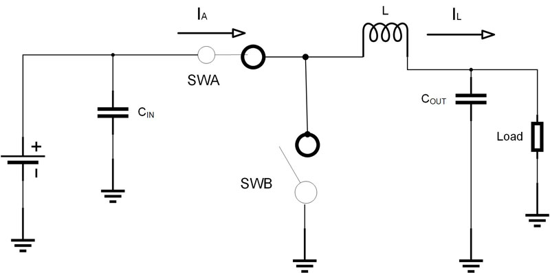
Figure 1: Basic Buck Converter Circuit (SWA Is On)
This article will discuss how to optimize input filter design for application boards that contain single or multiple DC/DC converters on the same voltage bus. An optimized input filter minimizes the cost and component count while ensuring circuit stability, provides EMI compliance, and improves input voltage transient response as well as output load transient response.
Overview
A well-designed input filter for a step-down DC/DC (buck) converter must achieve the following:
1. Create sufficiently low input impedance for the converter to maintain stability and prevent excessive input voltage (VIN) excursions during output load transients.
2. Attenuate high-frequency noise at the input terminals and prevent an injection of this noise into the ground plane or signal traces on the board.
3. Help attenuating any VIN spikes/transients that may be introduced by the input source or electromagnetic coupling of the external sources.
To achieve these goals, the designer must assess and understand circuit behavior, input supply, and environment characteristics.
Figure 1 shows a basic buck converter circuit and corresponding waveforms when SWA is on.
Figure 2 shows a basic buck converter circuit and corresponding waveforms when SWB is on.
Click image to enlarge
Figure 2: Basic Buck Converter Circuit (SWB Is On)
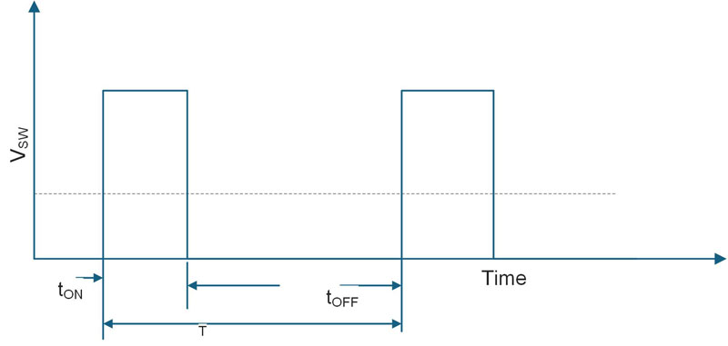
Figure 3 shows the converter’s switch node voltage waveform.
Click image to enlarge
Figure 3: Converter’s Switch Node Voltage Waveform
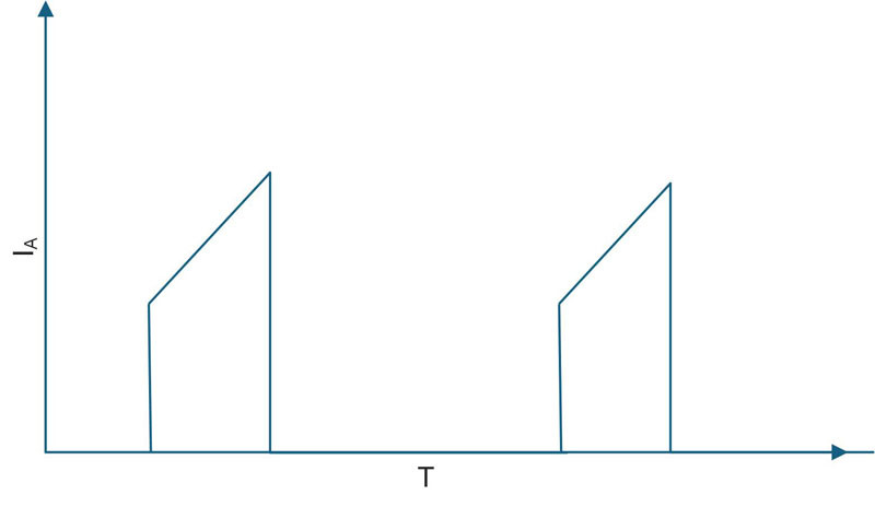
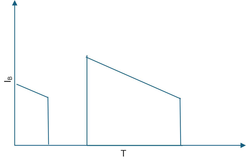
Figure 4 shows SWA’s current waveform.
Click image to enlarge
Figure 4: Converter’s SWA Current Waveform
Figure 5 shows SWB’s current waveform.
Click image to enlarge
Figure 5: Converter’s SWB Current Waveform
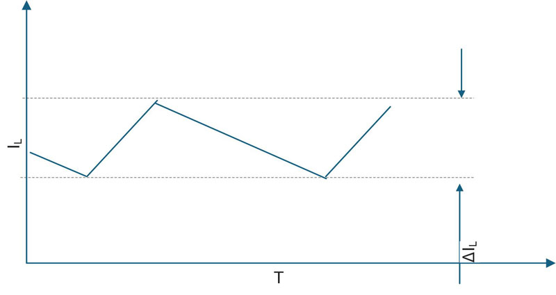
Figure 6 shows the converter’s output inductor current waveform.
Click image to enlarge
Figure 6: Converter’s Output Inductor Current Waveform
The physical design of the application board, type of input power source, and its connection to the DC/DC converter determine whether input inductors are required. If inductors are required, these parameters also determine which type of inductors (differential or common mode) should be used, as well as the appropriate impedance. However, even when no actual inductors are used, some parasitic inductance is always present because the transmission line characteristics add some impedance to the source supply’s output. This inherent parasitic inductance affects the behavior of the downstream DC/DC converter.
Goal 1: Low Input Impedance
To compensate for the impedance and accomplish the first goal for an input filter, designers must add bulk input capacitance to the DC/DC converter. The exact number of capacitors required in a specific design depends on the output load characteristics, the bandwidth of the converter, and the characteristics of the bulk capacitors being used (e.g. the capacitance including derating, equivalent series resistance (ESR), and equivalent series inductance (ESL)). It is also important to understand that bulk capacitors can typically be shared between several distinct power converters whose inputs are connected to the same input rail/bus.
The minimum acceptable input bulk capacitance (CIN_BULK) required to maintain the VIN excursions within a defined limit can be calculated with Equation (1):
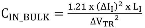
Where ΔII is the input current step, LI is the total input inductance, and ΔVTR is the maximum acceptable VIN deviation.
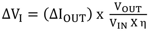
The input current step (II) is a function of the output current (IOUT) step, and it can be estimated with Equation (2):
The converter’s minimum input impedance of the converter can be calculated with Equation (3):
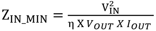
Where VIN is the input voltage, VOUT is the output voltage, IOUT is a steady state output current, and η is the converter’s efficiency.
It is important that the input filter does not have adverse effects on the stability of the switching supply. To accomplish this, the input filter must meet the Middlebrook criterion, which states that the switching supply’s input impedance must exceed the input filter’s output impedance.
Goal 2: Attenuate High-Frequency Noise
To minimize high-frequency noise and achieve the second goal, designers must typically use low-ESR ceramic capacitors at the input. The number of parallel capacitors required for the solution is determined by the capacitors’ ability to absorb input ripple current. The magnitude of the input ripple current can be estimated with Equation (4):
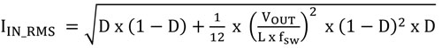
Where D is the converter’s duty cycle, L is the output inductance, VOUT is the output voltage, and fSW is the switching frequency.
It is also important to consider that ceramic capacitor characteristics are impacted by the DC bias, temperature, and their dielectric material composition. Designers cannot simply rely on the nominal capacitance and ESR values for these capacitors; designers should also verify how these values are affected by the operational conditions by studying the device’s datasheet.
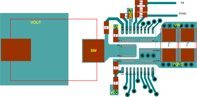
To ensure that these capacitors operate efficiently, it is important to minimize parasitic serial inductance between the input capacitors and converter’s IC terminals. Figure 7 shows an example of an optimized layout using the MP8796, a synchronous buck converter. The input capacitors (CIN1 and CIN2) are placed in the path at the input and return currents next to the IC input terminals. To attenuate the input ripple, these devices should be connected as close as possible to the upper FET drain and synchronous FET source with an additional capacitor (CIN3).
Click image to enlarge
Figure 7: Recommended Layout for the MP8796 Converter
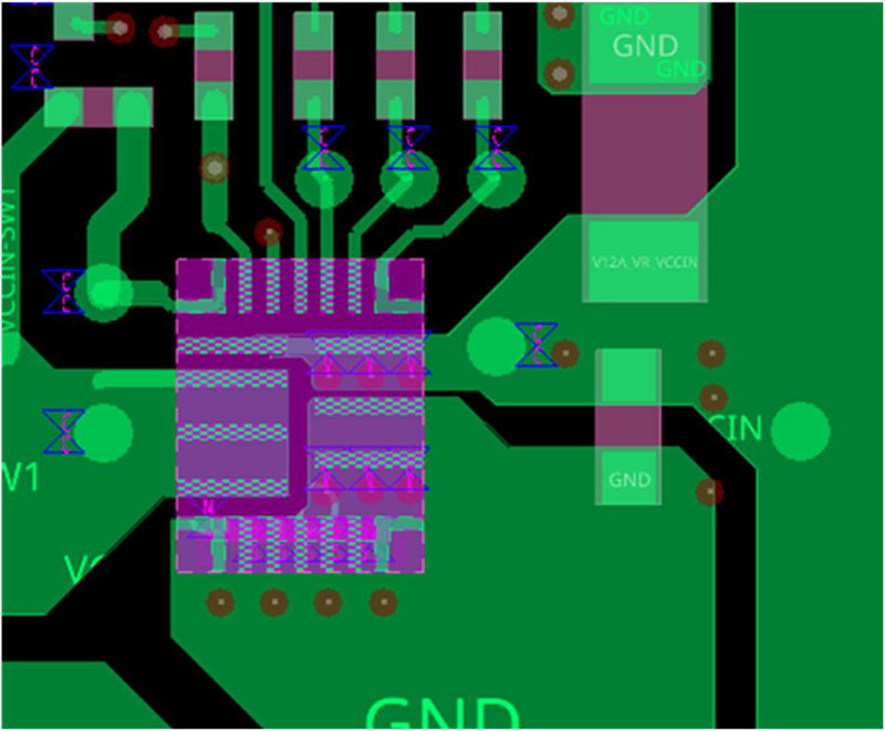
Figure 8 shows how the input capacitors can be placed ineffectively. Only one small ceramic capacitor (denoted in the red box) is placed efficiently with a minimum parasitic inductance. Meanwhile, other capacitors (denoted in the yellow box) are technically connected to the same node. The larger capacitors have more capacitance and a significantly higher parasitic inductance between their terminals and power converter terminals, which means that their impedance is too high to effectively filter out high frequencies.
It is also important to remember that the equivalent frequency of the input current waveform edges is significantly higher than a power converter’s fundamental fSW, which is typically ranges in the single to tens of MHz.
Click image to enlarge
Figure 8: Example of Application Layout of a Smart Power Stage
Goal 3: Attenuate VIN Spikes
To achieve the third goal and attenuate the VIN spikes, several measures must be considered during the design, depending on the design specifications and characteristics. To effectively attenuate VIN noise, follow the steps below:
Add common mode and differential filters (consisting of a combination of inductors and capacitors) at the input to suppress/attenuate any noise on the input terminals. Keep in mind that, as discussed earlier in the article, adding these filters increases the input impedance, which can impact the converter’s stability and dynamic behavior.
1. Consider the layout of the power traces on the board to minimize the parasitic loops. While the input terminals are connected through short traces with capacitors placed close to the converter terminals, input current return paths often meander through the board with input capacitors GND connections, forming large current loops that greatly reduce their effectiveness.
2. Treat ground planes as a part of the power structure rather than the equipotential point.
3. Keep switching nodes as short as possible and ensure that they are separated from any sensitive traces by GND and/or the power planes.
Conclusion
Designing the input filter for a switching power supply should follow a holistic approach and be carefully considered to help create a reliable, well-performing solution. There are three primary objectives when designing an input filter: creating a low input impedance, attenuating high-frequency noise, and minimizing VIN spikes.
This article described how to design an input filter for a switch-mode converter, such as the MP8796, that will save time, cut down on resources during the design verification stage, and result in improved overall performance. When these considerations are considered early in the process, a well-performing converter can be included in the board design without overdesigning and spending resources in the later stages. Explore MPS’s buck converter portfolio to find a solution for your needs.