GaN's Simplify Harmonic Reduction in High-Frequency Offline LED Drivers

This article describes how the use of GaN transistors can improve the total harmonic content of offline LED control gears
Figure 1: THD optimization model embedded in HVLED101
For more than a decade, solid-state lighting has become synonymous with lighting source. In fact, LEDs are used in almost every application field, including residential, outdoor, automotive and sanitization lighting. Smart algorithms have been developed to allow controllers to meet the requirements of dedicated standards written for lighting applications, especially for input power quality (IEC61000-3-2). The recent introduction of high-electron-mobility transistors (HEMTs) based on gallium nitride (GaN) in lighting applications not only improves efficiency and reduces size, but, as described in this article, can also improve the efficacy of total harmonic content reduction algorithms Input power quality is one of the most important parameters in this application field, and it is sometimes difficult to optimize.
Input Power Quality Optimization
According to the IEC61000-3-2, harmonic content in lighting applications must comply with the limits defined for the Class C. Historically, designers achieve this goal by adopting active power factor correction when the output power is greater than 25 W. The most frequently used topology to meet total harmonic content limits, safety constraints, and cost targets is the high-power-factor (HPF) flyback topology. It is a modified version of the traditional flyback topology in which the primary-side current is shaped synchronously with the input voltage. The flexibility of the flyback topology ensures proper operation of the LED power supply over a wide range of output voltages. This flexibility can permit a single-stage converter design.
Sinusoidal modulation of the peak primary-side current is apparently the simplest solution. However, theoretical analysis shows that, when it is applied to the HPF flyback topology, it cannot achieve zero total harmonic distortion (THD). In addition, when the converter operates over a wide output-voltage range, the THD increases at lower output voltages. The Equation 1 represents the input current value as a function of the phase (ϑ) of the sinusoidal input voltage. The term Ipkp is the maximum value of the peak current on the primary side, while |sin(ϑ)| is the sinusoidal modulation term. The operating duty cycle (δ), which is always lower than 1 and changes as a function of input voltage phase, indicates that the input current cannot be sinusoidal if the peak current on the primary side is modulated sinusoidally.
.jpg)
To improve the ability of the HPF topology to operate over a wide operating range, several total harmonic distortion (THD) optimization algorithms were developed. The most advanced algorithm is implemented in the HVLED101 controller by STMicroelectronics. It accurately detects the operating duty cycle and uses this value to cancel the correspondent term (δ(ϑ)) of Equation 2, by applying a shape to the envelope of the primary-side current peak (Equation 2). This method theoretically achieves zero THD for any input or output voltage condition.

The actual shape of the rectified sine wave in STMicroelectronics’ controller HVLED101 is read and scaled by the feedback voltage value that represents the output power demand. The signal then feeds the total harmonic distortion (THD) optimizer, which modifies the scaled half-sine-wave shape according to the operating duty cycle. As a result, the optimizer obtains the signal shape that modulates the peak of the primary-side current, which is measured across the shunt resistor. The operating duty cycle is computed from the primary-side switch conduction time and the secondary-side rectifier conduction time. The secondary-side rectifier conduction time is estimated from the signal generated across a dedicated winding of the flyback transformer. The computation assumes that the secondary-side current starts to flow after a negligible delay following the turnoff of the primary-side switch.
The algorithm demonstrates excellent performance on a 50 W LED control gear example, EVLHV101SSR50W. The total harmonic distortion (THD) remains below 10% over a power range from 100% to 33% of the nominal load, and below 25% at 10% of the nominal load.
Using GaN to Improve THD at Higher Operating Frequency
The primary-side switch of a flyback converter is selected by considering the maximum allowed drain-to-source voltage and the expected efficiency. However, when a high-power-factor (HPF) flyback converter is used, another parameter must be considered: drain-to-source capacitance. The nonlinear characteristic of the drain capacitance of the silicon MOSFET can affect the calculation of the operating duty cycle and, consequently, the effectiveness of the total harmonic distortion (THD) optimization term.
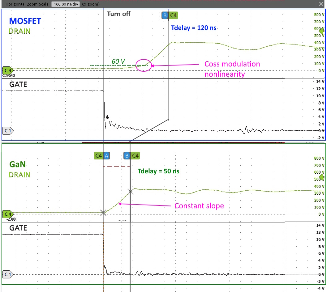
At MOSFET turnoff, the drain current starts to charge the drain-to-source parasitic capacitance (Coss) until the voltage across the primary side of the transformer is high enough to deliver energy to the output.
At low values of VDS, Coss is much higher than it is at high VDS. As a result, the VDS voltage does not increase linearly, and a delay occurs between primary-side switch turnoff and secondary-side energy deliveryThis delay creates a nonlinearity that the total harmonic distortion (THD) optimization algorithm cannot compute precisely. This delay affects operation of the THD optimizer when drain current is low and frequency is high, that is, when mains voltage is close to polarity inversion. High operating frequencies, for example from small transformers, make this operating condition more frequent.
When compactness is a key factor for the application, a higher operating frequency can be used with a different transformer. However, as mentioned above, THD measurably worsens, especially at low line.
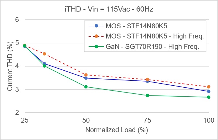
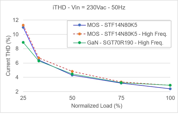
and Error! Reference source not found.illustrates the THD measurements for different solutions: the THD degradation is visible between MOSFET solution, indicated with blue curve, and MOSFET operating at high frequency, indicated with orange dotted curve.
Click image to enlarge
Figure 2: THD characterization of different system combinations at 115 Vac
Click image to enlarge
Figure 3: THD characterization of different system combinations at 230 Vac
The degradation can be reduced by using gallium nitride (GaN) transistors. High-electron-mobility transistor (HEMT) GaN transistors, because of their internal structure, offer a very small output capacitance (Coss) that does not exhibit Coss modulation at low VDS. As a result, VDS rises more linearly when the GaN transistor turns off (Error! Reference source not found.). The shorter delay time allows the total harmonic distortion (THD) algorithm to operate closer to theoretical conditions, especially near the mains zero crossings. A comparison was made with a GaN transistor (SGT70R190) that has the same energy-related Coss as the original MOSFET (STF14N80K5). An overall THD improvement is obtained (
and Error! Reference source not found., green curve).
Click image to enlarge
Figure 4: Comparison between slopes of MOSFET and GaN transistor at turn off of Flyback switch
Using GaN to Obtain Compact and Efficient Solution
The GaN used for this experiment shows a very low on-resistance (RDS(on)). As a result, power losses are very low at low input line. At high line, the equivalent drain capacitance is similar to that of the original MOSFET, so the switching losses caused by COSS are doubled. However, the smaller transformer size ensures lower parasitics that compensate for the higher switching losses.
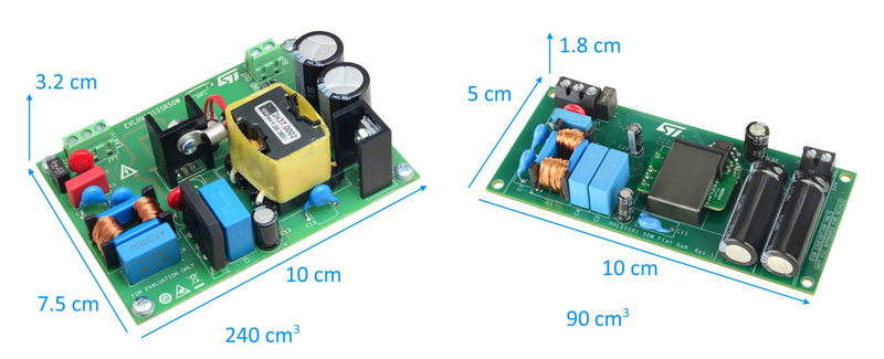
The combination of lower GaN RDS(on) and lower total drain capacitance permits the elimination of the large aluminum heatsink that the MOSFET originally uses. The efficiency of the GaN-based solution, which runs at double frequency, is practically the same as that of the MOS-based solution.
The overall volume decreases from 240 cm3 for the silicon MOS-based solution to 90 cm3 for the GaN-based solution, which is a reduction of more than 62%, as illustrated in Error! Reference source not found..
Click image to enlarge
Conclusion
The use of gallium nitride (GaN) transistors instead of silicon MOSFETs is commonly associated with increased efficiency and reduced size because of better dynamic performance and lower RDS(on) per area. This article shows the additional positive impact of adopting GaN transistors on the total harmonic distortion of a high-power-factor flyback converter used in lighting applications. The selection of the flyback power switch is rarely correlated with input power quality.
It has also been demonstrated that the use of GaN transistors in an LED power supply designed around a smaller transformer and operating at high frequency not only allows the removal of bulky heat sinks because of higher efficiency but also maintains very low total harmonic distortion and unity power factor over a wide range of input and output voltages.