Gate Driver Power Supply Challenges for SiC and GaN Devices

This article looks at the key considerations that must be made when designing power supplies for gate drivers in SiC and GaN applications
Figure 1: A few of the many RECOM DC/DC modules optimized for WBG gate driver applications
Silicon Carbide (SiC) and Gallium Nitride (GaN) are wide‑bandgap (WBG) semiconductor materials offering advantages over traditional silicon (Si) in power electronics because they switch faster with lower losses. They are gaining significant market share in applications where high efficiency and power density are critical. Early adopters vary by technology. SiC, the more mature technology, has largely replaced Si IGBTs for powering traction inverters in electric vehicles, while GaN has found success in laptop chargers and similar devices. However, GaN and SiC transistors are more difficult to drive than silicon MOSFETs, and gate driver power supplies for SiC and GaN devices must meet the specific bias requirements of these wide‑bandgap semiconductors.
What Are the Gate Driver Requirements for WBG Devices?
Gate drivers for SiC and GaN transistors must be matched to the device’s gate voltage limits, switching speed, and isolation requirements. High-side gate drivers require galvanic isolation for both the control signal and the DC/DC power supply. First-generation SiC MOSFETs typically require a +20V VDD gate drive during the on‑state to minimize on-resistance. Since the gate turn-on threshold can be less than 2V, SiC MOSFET drivers usually swing to a negative gate voltage during turn-off for optimal switching reliability.
SiC MOSFET and GaN HEMT circuit diagrams
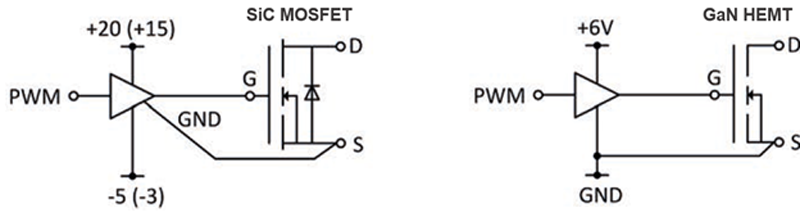
Click image to enlarge
Figure 2: Driver voltage comparison for SiC & GaN devices
Figure 2: Driver voltage comparison for SiC & GaN devices for next-generation devices, optimal turn-on and turn-off voltages are +15 or +18V and -3 or -4V, respectively. The gate driver must support very fast rise and fall times on the order of a few ns. Otherwise, most gate drivers can operate with asymmetric VDD and VEE supply voltages without issues. Gate driver power consumption increases with higher switching frequencies, but peak gate drive currents are supplied by capacitors placed close to the driver power supply pins, requiring only low power 2W to 3W DC/DC converters.
A GaN high electron mobility transistor (HEMT) has a typical full enhancement voltage of 7V but will be damaged if VGS exceeds 10V, much lower than SiC gate driver voltages. Due to the extremely fast rise and fall times of the HEMT’s low-capacitance gate channel, excessive inductance in the external gate drive can cause spikes or voltage ringing, exceeding safe limits. Therefore, a 6V gate drive voltage is a good compromise between high efficiency and safe operation. Unlike SiC MOSFETs, the HEMT gate channel’s low capacitance allows the turn-off voltage to be zero volts.
What Are the Key Specifications for WBG Gate Driver Power Supplies?
WBG gate driver power supplies must deliver the correct asymmetric gate voltages and provide robust galvanic isolation. Typical outputs are +20V / −5V for first-generation SiC MOSFETs, +15V / −3V for newer SiC devices, and +6V or +9V for GaN HEMTs. Because high-side gate drivers often operate hundreds of volts above ground, the DC/DC converter must provide isolation for the power supply itself in addition to control-signal isolation.
Basic isolation of a DC/DC converter may withstand 1kVDC for one second, but this is often insufficient for high-side gate drivers in bridge configurations. The DC/DC isolation voltage should be at least twice the working voltage. High ambient temperatures and fast switching from high-power SiC and GaN transistors add stress to the insulation barrier, necessitating highly isolated DC/DC converters for gate drivers.
Power Solutions for SiC and GaN Gate Drivers
RECOM’s DC/DC converters for gate drivers are drop-in modules providing reliable, long-life solutions for WBG applications. Our range of isolated DC/DC converter modules offers a simple power solution for SiC MOSFET or GaN HEMT devices. Features include asymmetric output voltages, high insulation voltage, and low isolation capacitance.
The following two RECOM DC/DC converter families are optimized for SiC and GaN gate driver technologies.
SiC MOSFETs
The RxxP22005 and RKZ-xx2005 series feature asymmetric outputs of +20V and -5V for efficient SiC MOSFET switching. The RxxP21503 series provides +15/-3V outputs, suitable for second-generation SiC MOSFETs.
GaN HEMTs
High slew-rate GaN transistor drivers achieve optimal switching at +6V using RECOM’s RP-xx06 and RxxP06 DC/DC converters, which offer high isolation voltage and low isolation capacitance. For higher noise or interference environments, RECOM also offers +9V output converters, which can be split via a Zener diode to +6V/-3V to provide negative gate voltage on turn-off, keeping gate voltage below the turn-on threshold.
Optimized for Gate Drivers
RECOM’s RA3 family of unregulated 3W DC/DC converters is specifically designed to power transistor gate drivers. Modules are available with 5, 12, or 24VDC input, with single or dual asymmetric outputs covering the latest Si, SiC, and GaN transistors. The compact SMD design minimizes board space, especially on multilayer PCBs. The modules offer 5.2kVDC/1min isolation and isolation capacitance under 10pF. Typical efficiencies of 78%–82% and an operating range of -40°C to +85°C at full load meet demanding requirements for solar inverters, induction heating, telecom, EV battery chargers, and motor drives.
Futureproofing WBG Designs
Click image to enlarge
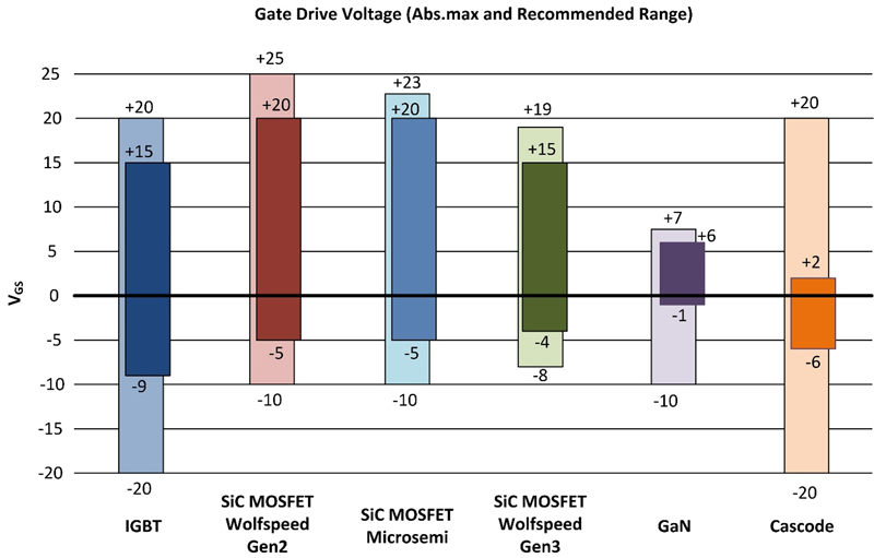
Figure 3: Recommended and absolute maximum driver voltage comparison for different IGBT, SiC & GaN devices
The optimal gate driver supply voltage varies by transistor type (IGBT, SiC, GaN), manufacturer, technology generation, and whether a cascode configuration is used. This creates concerns for electronics designers: how can designs accommodate future generations or alternate transistor suppliers with different optimal turn-on and turn-off voltages?
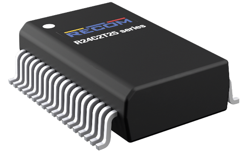
RECOM’s R24C2T25 converter addresses this challenge. This isolated SMD DC/DC converter in an IC-style SSOP package is designed for isolated WBG gate drivers. The regulated positive and negative outputs can be independently adjusted from +2.5V to +22.5V / -2.5V to -22.5V using preset resistors, covering all existing gate driver voltages for IGBT, MOSFET, SiC (all generations), or GaN with a single part (Figure 4).
The output is Basic Grade isolated to 3kVrms/1min and delivers 1.5W across -40°C to +105°C without derating (2W up to +85°C). CMTI (Common Mode Transient Immunity) exceeds 150kV/µs, making it suitable for very fast switching edges. The SMD SSOP package can be mounted close to switching transistors, and outputs are fully protected (UVLO, OTP, SCP, OLP) for safe, worry-free installation.
Click image to enlarge
Figure 4: R24C2T25 adjustable asymmetric output voltage gate driver power supply
Conclusion
Wide‑bandgap transistors offer unique advantages in high-power applications but challenge designers of SiC and GaN gate driver power supplies. Standard DC/DC isolation is insufficient for these circuits, requiring specialized solutions. RECOM integrates high insulation voltage, asymmetric outputs, and low isolation capacitance into several DC/DC module families optimized for SiC and GaN gate driver designs.