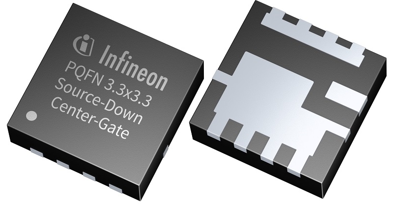
Infineon has launched the OptiMOS 40 V low-voltage power MOSFET to the market.
It is packaged in the Source-Down (SD) PQFN with a 3.3 x 3.3 mm2 footprint. The 40 V SD MOSFET primarily addresses SMPS for server, telecom, and OR-ing, as well as battery protection, power tool, and charger applications.
The SD package features silicon that is being flipped upside down inside of the component. With that, the source potential is connected to the PCB over the thermal pad instead of the drain potential. In the end, this variant can lead to a major reduction of R DS(on) by up to 25 percent compared to the current technology. The thermal resistance between junction to case (R thJC) is also significantly improved compared to the traditional PQFN packages. The SD OptiMOS can withstand high continuous currents of up to 194 A. Additionally, the optimized layout possibilities and the more efficient utilization of the PCB allow for greater design flexibility together with highest performance.
Availability
The OptiMOS SD 40 V low-voltage power MOSFET is available in two versions, standard and Center-Gate. The Center-Gate variant is optimized for parallel operation of multiple devices. Both variants in the PQFN 3.3 x 3.3 mm2 package can be ordered now.