Using Early EMI Testing to Validate SiC-based Designs
Silicon carbide’s (SiC) unique characteristics make it a popular replacement for silicon (Si) in many applications
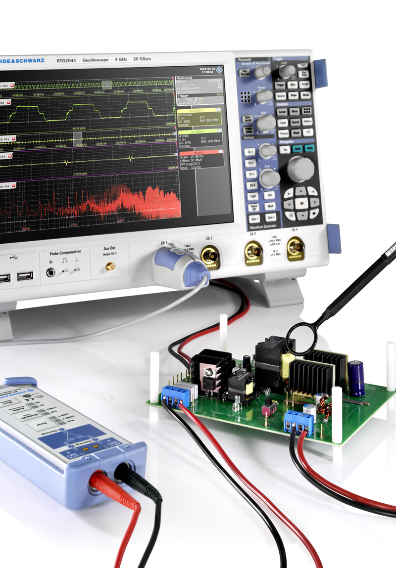
Figure 1. Probing a power design with a real-time oscilloscope can help identify the sources and transmission paths of unwanted emissions
In applications like automotive, green energy, and data centers, the primary growth drivers for SiC are potential gains in performance, efficiency and power density. However, the gains in performance and size must still run the gauntlet of faster switching speeds, large currents, and issues related to new packaging requirements.
While the move to SiC has its advantages, designing on silicon is cheap and well-understood. Consequently, the path to SiC adoption has faced a couple of key hurdles. First up was a hiccup in failing to meet operational requirements in harsh-environment applications outlined in qualifications such as HV-H3TRB. After some early reliability concerns, SiC devices have demonstrated higher withstand voltages, surpassing the 1,000 hours of required high-temperature, high-humidity bias testing. The second, and parallel, challenge has been cost. Many designs are under considerable cost restrictions, but SiC devices are delivering on the promise of price-performance expectations.
More recently, the conversation has changed from the theoretical to the practical. No one can dispute SiC’s performance and environmental values on a data sheet; however, it’s likely that SiC isn’t a simple drop-in replacement for silicon. There are new learning curves for optimizing the design and addressing issues related to packaging. Noise has surfaced as a potential limitation.
Faster switching speeds, system parasitics, and board layout increase the urgency for electromagnetic interference(EMI) pre-compliance testing. Testing your SiC design to make certain it isn’t noisy compared to silicon requires EMI testing to be performed early and often. The good news: a power designer doesn’t have to become an EMC test expert to perform valid and useful pre-compliance tests on SiC devices.
This article offers an overview of EMI basics and discusses essential test tools and methods. These points are the foundation of a case study that compares EMI test results for a switched-mode power supply (SMPS) that ships with Si MOSFETs and to those measured from the same SMPS modified with SiC MOSFETs.
EMI Basics and Potential Causes
EMI is unwanted coupling of interference signals from one circuit to another or to an entire system. There are two forms of EMI: radiated and conducted. Radiated EMI occurs over the air through radio-frequency (RF) emissions. Conducted EMI is typically coupled in one of three ways: parasitic impedances, component-to-component connections, or connections to ground.
In power electronics, four areas of concern are directly related to the potential for EMI:
· Parasitic inductance around the power device and its load
· Inductance at the gate, which can be part of the drive circuit or the package
· Coupling between the gate drive and the power device (and load)
· Coupling between the traces in the SiC module substrate and the baseplate (which has a small capacitance)
Stray inductance is especially problematic in designs that utilize fast switching speeds at high voltages and currents. These conditions give rise to higher dv/dt and di/dt, and just a few nanohenries of stray inductance can cause problematic voltage drops.
In addition, faster switching speeds produce larger displacement currents. Current flow can occur through any conductive pathway, including enclosures, mounting brackets or fasteners. Large spikes in displacement current can be injected into the module’s heatsink due to the large dv/dt present at the output.
In the power stages, excess inductance can also lead to switching overshoot, undershoot and oscillations (i.e., ringing). Oscillations are especially troublesome because they increase the likelihood of coupling (radiated or conducted).
Test Tools and Accessories
Fortunately, sound EMI measurement techniques will accelerate the process of finding, fixing and validating SiC devices and systems. For power designers, frequent EMI “checkups” help in three ways:
· Identify sources of unwanted emissions
· Provide information that supports problem mitigation and design optimization
· Increase the likelihood of passing full compliance testing
Before sending a design out for formal verification, it’s extremely critical to conduct pre-compliance testing in the lab. As luck would have it, a lot of insights can be gained using an instrument found on most benches—an oscilloscope (Figure 1).
To enable the necessary frequency-domain measurements, it’s recommended to use an oscilloscope with sufficient performance (1 GHz and higher) equipped with fast Fourier transform (FFT) capabilities, FFT gating, and frame overlay processing (to compensate for FFT windowing functions). You also want an instrument with low noise and high input sensitivity to enhance the ability to detect and analyze weak emissions.
Another recommended tool is EMI pre-compliance software such as the RTx Pre-Compliance Software from Rohde & Schwarz (R&S). Programmed with specific procedures and test limits from relevant international standards, the software simplifies testing and analysis for non-specialists. For example, the software provides fast, easy-to-interpret results and creates an environment that ensures repeatable testing. An example of using a scope with this software is shown in the following case study.
EMI Case Study: Comparing SiC to Si
Recently, Wolfspeed, a leading manufacturer of SiC power solutions, collaborated with R&S to determine if replacing Si MOSFETs with readily available SiC MOSFETs would cause an increase in system noise. The test specimen was an off-the-shelf SMPS.
Separate sets of EMI measurements were performed with both Si and SiC MOSFETs installed in the SMPS. Measurements were made using an R&S real-time oscilloscope, nearfield probes, a line impedance stabilizer network (LISN), and R&S pre-compliance test software. The goal was to pass a specific certification test that applies to electrical and electronic apparatus used in industrial environments (e.g., EN61000-6-4, class B).
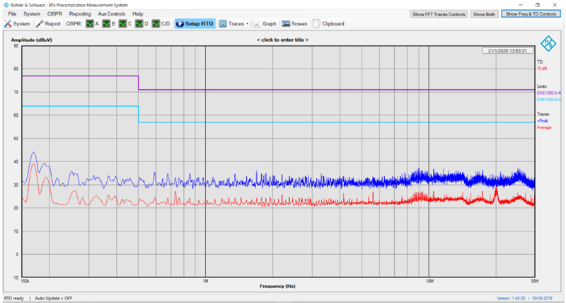
Baseline testing was performed with the Si MOSFETs installed on a unit that had previously passed compliance testing. As shown in Figure 2, the measured results were well below the test limits (purple and light-blue lines).
Click image to enlarge
Figure 2. For the proven Si-based design, the peak (blue) and average (red) results would easily pass EMI testing
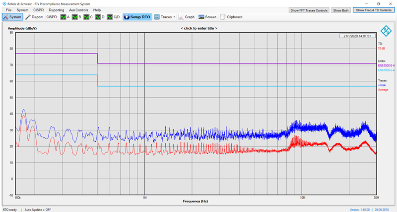
Next, the Si MOSFETs were replaced with SiC transistors. In both cases, relevant mitigation and optimization techniques were applied. Figure 3 shows the test results for a TO-247-3 configuration. As with the Si MOSFET, the results were well below the limits, indicating the readiness of this design for EMC compliance testing.
Click image to enlarge
Figure 3. Replacing the Si MOSFETs with SiC MOSFETs as TO-247-3, the results are well below required limits
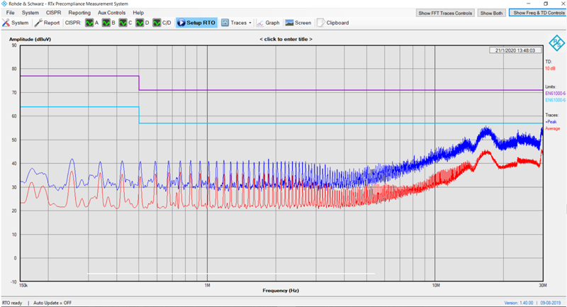
Figure 4 shows the test results after re-configuring the package as TO-247-4. Once again, the results were below the test limits: with more than 10 dBµW of margin between the average value (red) and the light-blue limit line, this version would also pass emissions testing.
Click image to enlarge
Figure 4. Re-configuring the package as TO-247-4, the results are still well below limits with more than 10 dBµW margin
Conclusion
Design trends suggest SiC will continue to prove its value in high-power designs: EVs, solar inverters, data center UPS, and more. Removing noise as a barrier to entry has been made more straightforward using an oscilloscope, task-specific software, and the necessary test accessories.
With these tools, power designers can identify EMI sources, apply necessary mitigation, and further optimize their designs as part of their day-to-day work. In many cases, the migration from Si to SiC will require only modest amounts of mitigation to keep EMI levels well within the specified limits.


