There is a simple method of switching between the external +5V supply and a rechargeable single-cell Lithium-ion (Li+) battery
Some portable applications need to be powered up from an external +5V wall adapter supply and still require a +5V system voltage when in battery-backup mode. This design provides a simple method of switching between the external +5V supply and a rechargeable single-cell Lithium-ion (Li+) battery. The design will still maintain uninterrupted +5V to the application circuitry.
Three key circuit functions are needed:
1. An efficient Li+ battery charger
2. An efficient boost converter to convert the battery voltage to +5V
3. A low-loss switchover circuit that automatically switches between the main DC power and the backup Li+ battery
As shown in Figure 1, U1 is a high-performance battery charger (MAX8903) capable of supplying up to 2A to charge a single-cell battery. Resistors RIDC and RISET set the DC-input current limit and charge-current set points, respectively. Since the SYS output (pins 23 and 24) is not used, the charge current will be constant and not dictated by the load current.
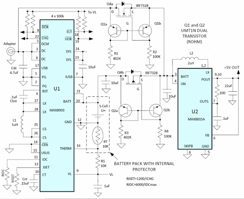
Click image to enlarge
Figure 1. This design switches between the external +5V supply and a rechargeable single-cell Li+ battery to provide a constant +5V output.
Q1 and Q2 are dual PNP transistors, available in an SC74 package. These transistors are used with the p-channel FETs, Q4a and Q4b, to form ideal low-loss ORing diodes. The output of the ORing diode configuration is then fed to a high-efficiency boost converter, U2 (MAX8815A). When the +5V input voltage is present, U1 is charging the battery. Q4a conducts, as the voltage on R2 provides a negative bias with respect to Q4a source voltage. The voltage on the base of Q2b is higher than the voltage on the emitter of Q2a transistor. Consequently, Q2a is turned off and Q2b is turned on because enough base current flows thru R3 to ground. Since Q2b is now fully on, the voltage at the Q2b collector is very close to the output voltage. Q4b is also biased off as the voltage difference between its gate and source pins are close to zero. When the +5V source is removed or lower than the battery voltage, circuit operation is identical to the above description for Q4b, Q1a, Q1b, R4, and R1.
U2 is a highly efficient boost converter that delivers over 1A of continuous current. As the input voltage to U2 has a range of 3.0V to 5V, U2 still provides a highly regulated 5V output even when the input is +5V.1
There are advantages and disadvantages to placing the boost in the power path of the +5V wall adapter. The disadvantage is with the efficiency. The boost converter will incur more power losses versus a circuit that simply uses a FET switchover circuit to switch between the wall adapter voltage and the boosted battery voltage. There is, however, a nice advantage of using a boost at the output: it will regulate the +5V output and account for IR drops in the adapter cable. Additionally, placing the MAX8815A at the output provides short-circuit protection.
Figure 2 shows a way to implement this circuit with fewer parts. This approach uses the SYS output of the MAX8903 as the input to the MAX8815A boost converter. This method eliminates transistors Q1 and Q2 as the switching elements, and uses the internal switchover circuit of the MAX8903.
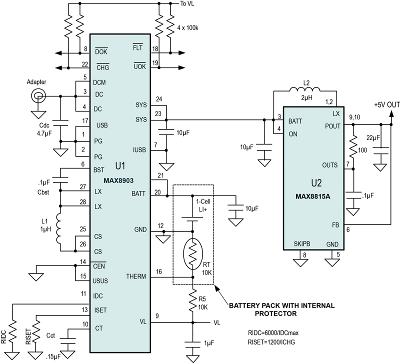
Click image to enlarge
Figure 2. This design also switches between the external +5V supply and a rechargeable single-cell Li+ battery to provide a constant +5V output.
Lowering the part count comes with trade-offs. The main performance drawback to this approach is lower efficiency. When the main input is connected, the MAX8903 regulates the output to 4.4V or 4.325V depending on the part variant. When the battery voltage is at the VCHG point, the voltage regulates the SYS output to one of these voltages. A second trade-off is with the battery charge current—it is load dependent. This means that the charge current is the difference between the input current limit, which is settable up to 2A, and the load current. As such, at full output load it will take a longer time to charge the battery versus when the output is lightly loaded.
There is, finally, a good advantage to this approach: the input operating range of the MAX8903. The input voltage range is specified 4.5 to 16V with 20V input protection. The circuit in Figure 1 is limited by the 5.5V maximum operating input voltage of the MAX8815A.


