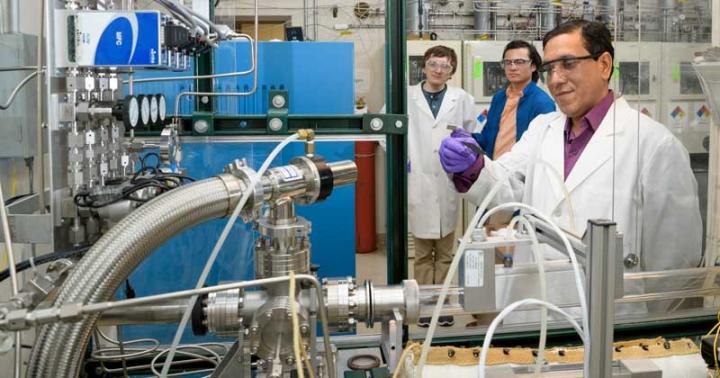
Ujjwal Das, an associate scientist at the University of Delaware's Institute of Energy Conversion, examines a silicon wafer after a thin layer of sulfur - less than 5 nanometers thick - was deposited on the surface. In the background, doctoral students Robert Theisen and Isaac Lam watch a silicon wafer emerge from the atmospheric pressure vapor treatment reactor, where it was treated with hydrogen sulfide and hydrogen selenide gases. The reactor was developed at IEC.


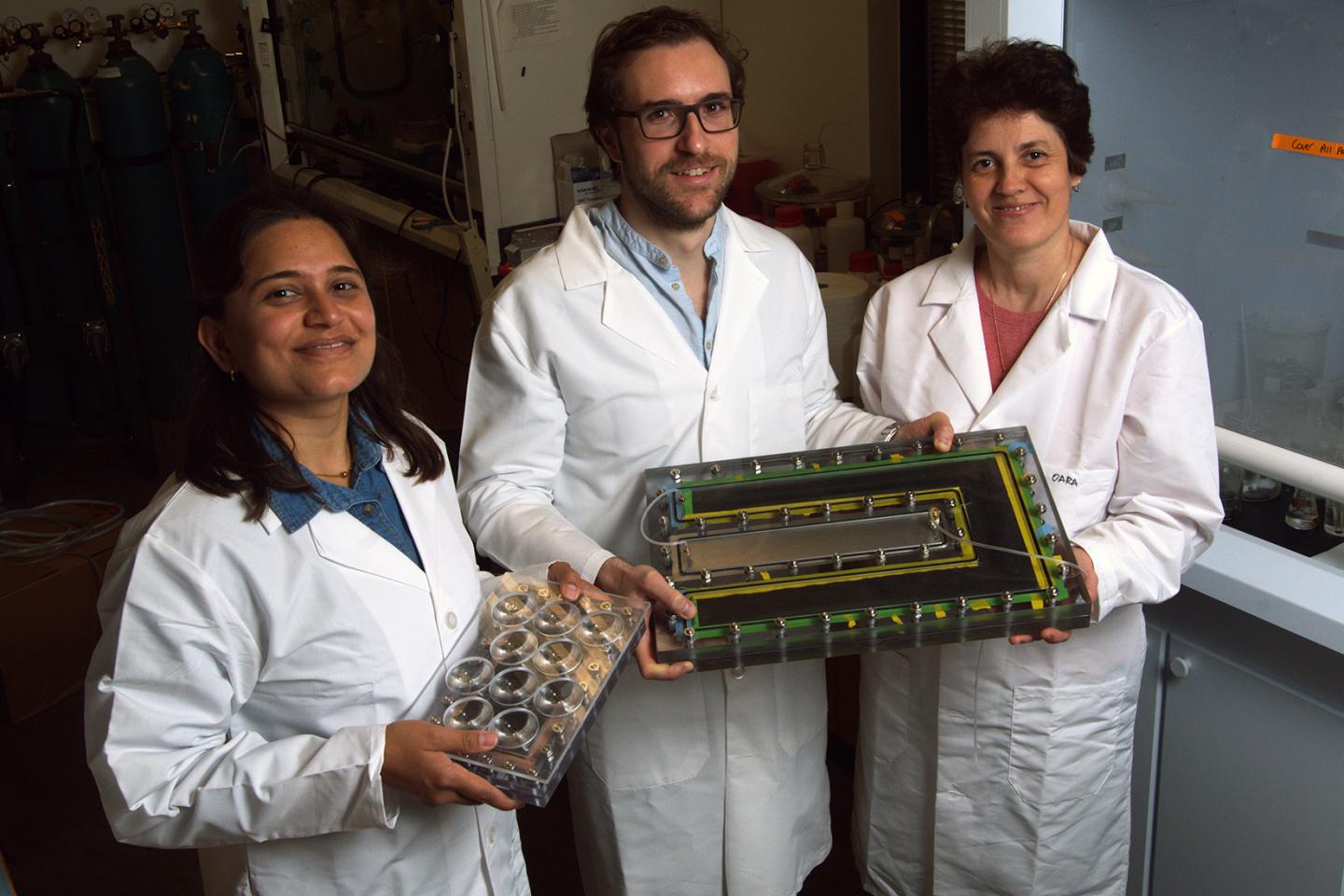
Rice University researchers (from left) Pratiksha Dongare, Alessandro Alabastri and Oara Neumann showed that Rice's 'nanophotonics-enabled solar membrane distillation' (NESMD) system was more efficient when the size of the device was scaled up and light was concentrated in 'hot spots.'
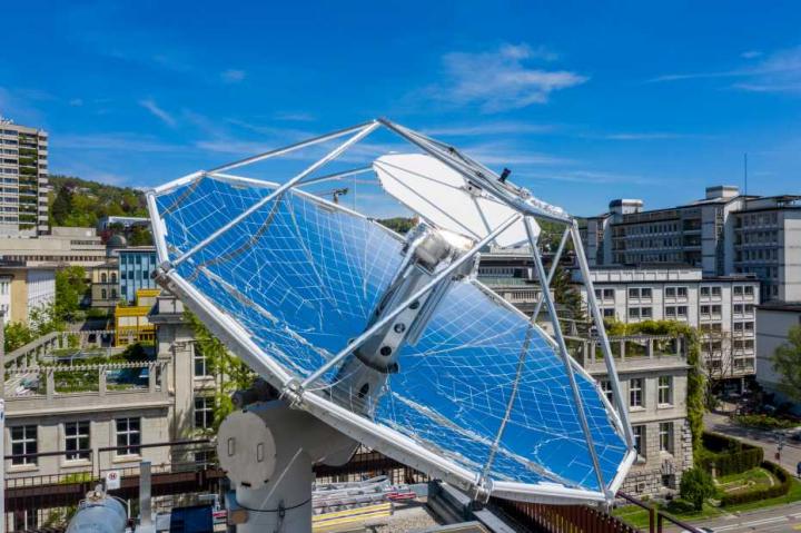
The research plant is located on the roof of the ETH building on Sonneggstrasse.

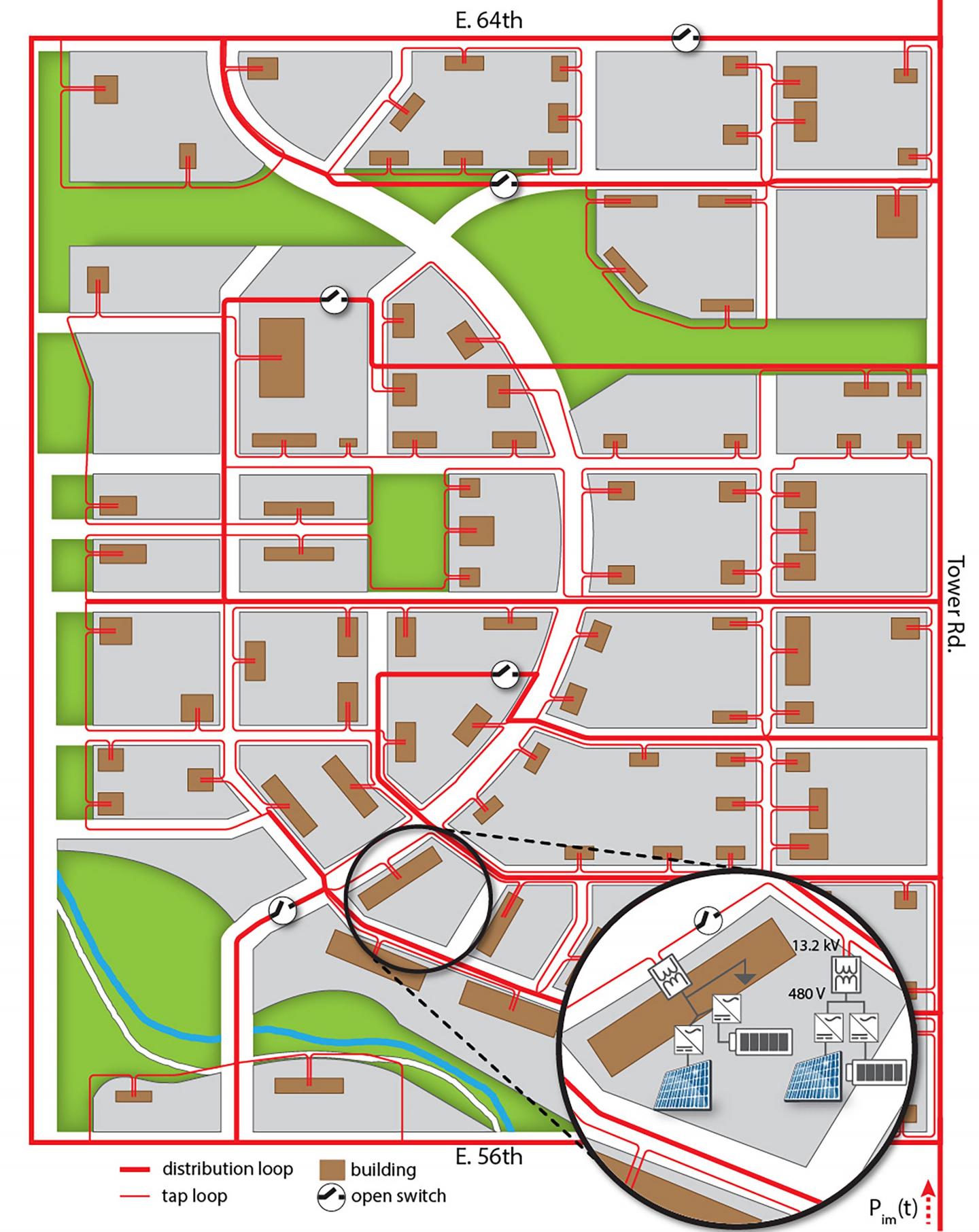
Researchers are using advanced modeling and visualization tools to help create the planned net-zero energy district, Peña Station NEXT, near the Denver International Airport in Denver, Colorado.